


How Does the Wafer Mounting Plate Lay the Precision Foundation of Chip Manufacturing?
Release Time : 2026-03-19
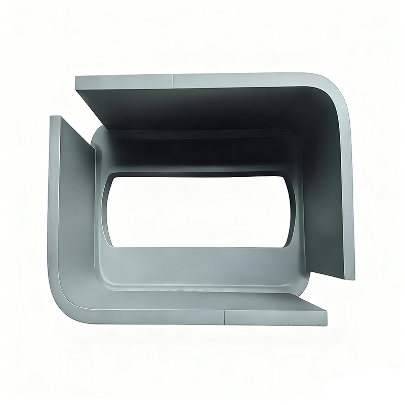
In the grand scheme of the semiconductor industry, the wafer, as the substrate carrying integrated circuits, has near-obsessive precision requirements in its manufacturing and processing. At the very beginning of this precision chain, the wafer mounting plate plays a crucial role. This seemingly simple platform is actually a key bridge connecting the microscopic world of chips to macroscopic manufacturing equipment. Its performance directly determines the success or failure of core processes such as photolithography, dicing, and grinding, making it an indispensable precision foundation of the modern electronics industry.
The core mission of the wafer mounting plate is to provide ultimate flatness and stability. In nanoscale processes, any tiny undulation or vibration on the wafer surface can lead to misalignment of circuit patterns or even scrapping. High-performance mounting plates are made of special ceramics, Invar alloys, or high-strength aluminum alloys that have undergone special heat treatment. These materials have extremely low coefficients of thermal expansion, enabling them to withstand heat fluctuations generated during processing and ensuring dimensional stability even under drastic temperature changes. Through ultra-precise grinding and polishing processes, the surface of the mounting plate achieves atomic-level flatness, enabling a tight fit between ultra-thin wafers and eliminating the risk of warping or cracking due to uneven stress. This creates a perfect physical foundation for subsequent microfabrication.
Excellent thermal management is another key indicator of a wafer mounting plate. During high-speed cutting or high-energy laser processing, large amounts of heat can be generated instantaneously in localized areas. If this heat cannot be dissipated in time, it can easily cause thermal damage to the wafer or alter its material properties. Advanced mounting plates incorporate complex microchannel cooling systems or utilize highly thermally conductive composite materials to rapidly and evenly diffuse and remove heat, maintaining a constant overall wafer temperature. This efficient heat conduction mechanism not only protects the fragile chip structure but also significantly improves processing speed and yield, enabling the smooth implementation of high-power, high-density manufacturing processes and meeting the urgent demand for high-performance chips in modern electronic products.
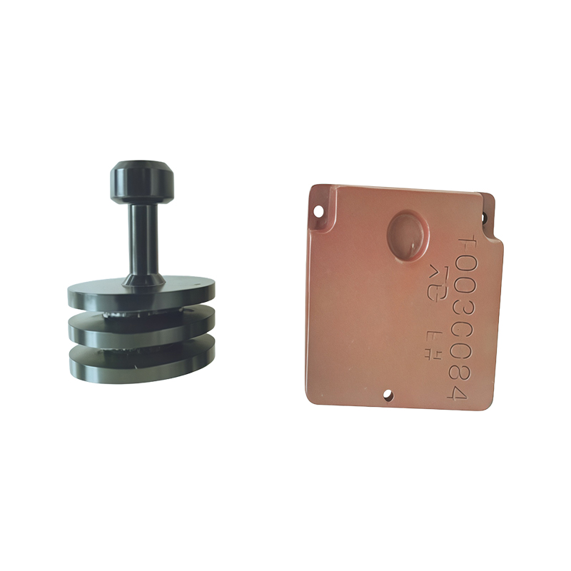
Electrostatic discharge (ESD) protection and cleanliness control are also paramount in wafer mounting plate design. Semiconductor manufacturing requires extremely high environmental cleanliness; even tiny dust particles or electrostatic adsorption can cause short circuits. Mounting plates typically undergo a special anti-static coating or utilize intrinsically anti-static materials, effectively eliminating static electricity buildup and preventing dust adsorption or electrostatic discharge damage to wafers during transport and mounting. Simultaneously, their structural design eliminates dead corners and gaps, facilitating cleaning and maintenance, and meeting high-level cleanroom standards. This rigorous control over the microscopic environment ensures that each wafer is manufactured in a pure and contamination-free environment, guaranteeing the reliability of the final product.
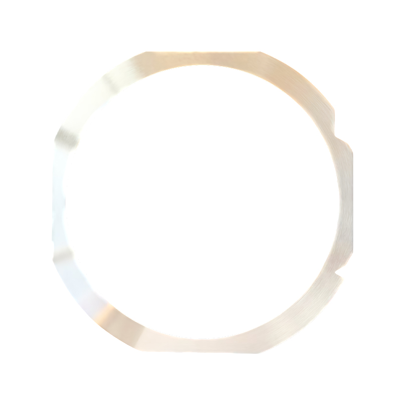
Compatibility and automation adaptability make wafer mounting plates flexible nodes in intelligent manufacturing processes. As wafer sizes evolve from eight inches to twelve inches and even larger, mounting plates must possess highly standardized interfaces and precise positioning mechanisms to adapt to different models of pick-and-place machines, dicing machines, and inspection equipment. Precision positioning pin holes and vacuum suction groove designs enable rapid wafer clamping and precise alignment, which, combined with automated robotic arm operations, significantly shortens production cycle time. This high degree of compatibility not only enhances the flexibility of the production line but also reduces changeover costs, making large-scale mass production more efficient and smooth.
From smartphone processors to AI accelerator cards, every high-performance chip relies on the silent support of a wafer mounting plate. With its extreme precision, stable thermal control, robust protection, and efficient adaptation, it safeguards every minute detail of semiconductor manufacturing. As Moore's Law continues to drive technological iteration, technological innovation in wafer mounting plates has never ceased. The application of new materials and the exploration of new structures constantly push the limits of physics. It is not only the physical platform that carries the wafer, but also an invisible engine propelling electronic technology forward, building the foundation of a grand digital civilization in the microscopic world and leading human technology towards a more intelligent and interconnected future.
The core mission of the wafer mounting plate is to provide ultimate flatness and stability. In nanoscale processes, any tiny undulation or vibration on the wafer surface can lead to misalignment of circuit patterns or even scrapping. High-performance mounting plates are made of special ceramics, Invar alloys, or high-strength aluminum alloys that have undergone special heat treatment. These materials have extremely low coefficients of thermal expansion, enabling them to withstand heat fluctuations generated during processing and ensuring dimensional stability even under drastic temperature changes. Through ultra-precise grinding and polishing processes, the surface of the mounting plate achieves atomic-level flatness, enabling a tight fit between ultra-thin wafers and eliminating the risk of warping or cracking due to uneven stress. This creates a perfect physical foundation for subsequent microfabrication.
Excellent thermal management is another key indicator of a wafer mounting plate. During high-speed cutting or high-energy laser processing, large amounts of heat can be generated instantaneously in localized areas. If this heat cannot be dissipated in time, it can easily cause thermal damage to the wafer or alter its material properties. Advanced mounting plates incorporate complex microchannel cooling systems or utilize highly thermally conductive composite materials to rapidly and evenly diffuse and remove heat, maintaining a constant overall wafer temperature. This efficient heat conduction mechanism not only protects the fragile chip structure but also significantly improves processing speed and yield, enabling the smooth implementation of high-power, high-density manufacturing processes and meeting the urgent demand for high-performance chips in modern electronic products.
Electrostatic discharge (ESD) protection and cleanliness control are also paramount in wafer mounting plate design. Semiconductor manufacturing requires extremely high environmental cleanliness; even tiny dust particles or electrostatic adsorption can cause short circuits. Mounting plates typically undergo a special anti-static coating or utilize intrinsically anti-static materials, effectively eliminating static electricity buildup and preventing dust adsorption or electrostatic discharge damage to wafers during transport and mounting. Simultaneously, their structural design eliminates dead corners and gaps, facilitating cleaning and maintenance, and meeting high-level cleanroom standards. This rigorous control over the microscopic environment ensures that each wafer is manufactured in a pure and contamination-free environment, guaranteeing the reliability of the final product.
Compatibility and automation adaptability make wafer mounting plates flexible nodes in intelligent manufacturing processes. As wafer sizes evolve from eight inches to twelve inches and even larger, mounting plates must possess highly standardized interfaces and precise positioning mechanisms to adapt to different models of pick-and-place machines, dicing machines, and inspection equipment. Precision positioning pin holes and vacuum suction groove designs enable rapid wafer clamping and precise alignment, which, combined with automated robotic arm operations, significantly shortens production cycle time. This high degree of compatibility not only enhances the flexibility of the production line but also reduces changeover costs, making large-scale mass production more efficient and smooth.
From smartphone processors to AI accelerator cards, every high-performance chip relies on the silent support of a wafer mounting plate. With its extreme precision, stable thermal control, robust protection, and efficient adaptation, it safeguards every minute detail of semiconductor manufacturing. As Moore's Law continues to drive technological iteration, technological innovation in wafer mounting plates has never ceased. The application of new materials and the exploration of new structures constantly push the limits of physics. It is not only the physical platform that carries the wafer, but also an invisible engine propelling electronic technology forward, building the foundation of a grand digital civilization in the microscopic world and leading human technology towards a more intelligent and interconnected future.