
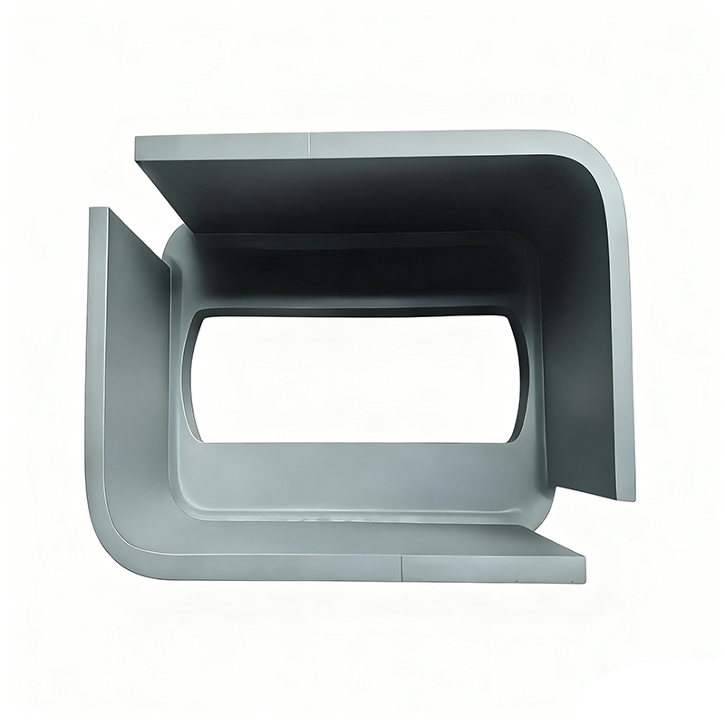


In the design of electronic wafer mounting plates, how can structural optimization simultaneously meet the requirements of high heat dissipation and low thermal expansion coefficient?
Release Time : 2025-11-19
With the rapid development of semiconductor processes towards higher integration and smaller linewidths, the heat density generated by electronic wafers during operation has increased dramatically, posing unprecedented challenges to the thermal management capabilities of mounting substrates. Simultaneously, to avoid mechanical stress or even cracking between the wafer and substrate caused by temperature changes, the wafer mounting plate must also possess extremely low thermal deformation characteristics.
1. Multilayer Composite Structure: Functional Partitioning Achieves Performance Synergy
A single material cannot simultaneously meet the requirements of high thermal conductivity and low thermal deformation. For example, while copper has excellent thermal conductivity, it expands significantly when heated; ceramics have good stability, but limited thermal conductivity. Therefore, modern wafer mounting plates generally adopt a multilayer composite structure design. A typical solution is to embed microchannels or heat diffusion layers made of highly thermally conductive metals onto a high-rigidity, low-deformation ceramic or silicon carbide substrate. This "rigid-flexible" structure allows heat to be rapidly conducted from the wafer to the heat dissipation path, while the overall framework is dominated by low-expansion materials, effectively suppressing macroscopic deformation. By precisely controlling the thickness of each layer and the bonding strength at the interface, an optimal balance between thermal performance and dimensional stability can be achieved without sacrificing flatness.
2. Microstructured Heat Dissipation Channels: Enhancing Heat Transfer Efficiency
To further strengthen heat dissipation capabilities, engineers integrate micron-level flow channels or fin arrays within the mounting plate. These microstructures significantly increase the heat exchange area and can interface with external liquid cooling systems to form an active heat dissipation loop. For example, in the mounting plates of high-power lasers or RF chips, laser etching or electrochemical processing techniques are often used to construct a three-dimensional interconnected cooling network within the metal layers. Coolant flowing through this network quickly removes heat, maintaining the wafer's operating temperature within a safe range. Simultaneously, the microchannel layout is optimized through fluid dynamics simulation to ensure uniform flow and reasonable pressure drop, avoiding localized overheating or structural stress concentration, thus ensuring efficient heat dissipation while maintaining controllable overall deformation.
3. Interface Optimization and Stress Buffer Design
The interface between the wafer and the mounting plate is the area where thermal stress is most likely to concentrate. To mitigate this problem, flexible transition layers or lattice support structures are often introduced in the design. For example, using nano-silver sintered layers or highly thermally conductive flexible adhesives in critical connection areas ensures good heat conduction while allowing for minor deformation to absorb strain caused by thermal mismatch. Furthermore, some high-end products incorporate stress-relieving grooves or honeycomb-shaped perforations at the edges of the mounting plate, guiding deformation direction through localized weakening and preventing stress transmission to the wafer center. This "rigid yet flexible" design philosophy significantly improves system reliability under repeated thermal cycling.
4. Precision Manufacturing Ensures Design Implementation
Even the best structural design relies on high-precision manufacturing processes. We can customize and develop wafer mounting plates according to customer needs, equipped with advanced CNC machining centers, vacuum brazing equipment, and ultra-precision surface grinders to ensure micron-level dimensional tolerances and sub-micron-level surface flatness. Simultaneously, high-resolution X-ray inspection, infrared thermal imaging, and 3D topography analyzers are used to comprehensively verify the thermal performance and geometric accuracy of each batch of products, ensuring their stable performance in practical applications while maintaining high heat dissipation and low deformation advantages.
In the field of advanced electronic packaging, the wafer mounting plate is not only a load-bearing platform but also a core hub for thermal management and structural stability. Through the deep integration of composite material architecture, microscale heat dissipation channels, intelligent stress buffering and precision manufacturing processes, modern mounting plates have successfully achieved synergistic optimization of high thermal conductivity and low thermal deformation.