


Can wafer mounting plates achieve nanometer-level precision and reliable process support in advanced semiconductor manufacturing?
Release Time : 2025-11-07
In the precision world of semiconductor manufacturing, even a nanometer-level deviation can determine the success or failure of chip yield. As a core tooling component that temporarily supports and positions the wafer during critical processes such as etching, deposition, inspection, and bonding, the wafer mounting plate, while not directly involved in circuit formation, plays a decisive role in the stability, repeatability, and cleanliness of the entire process. Its performance not only affects equipment operating efficiency but also directly impacts wafer surface integrity and device electrical characteristics. Therefore, high-end wafer mounting plates must meet near-stringent standards in multiple dimensions, including geometric accuracy, material properties, conductivity control, and cleanliness levels.
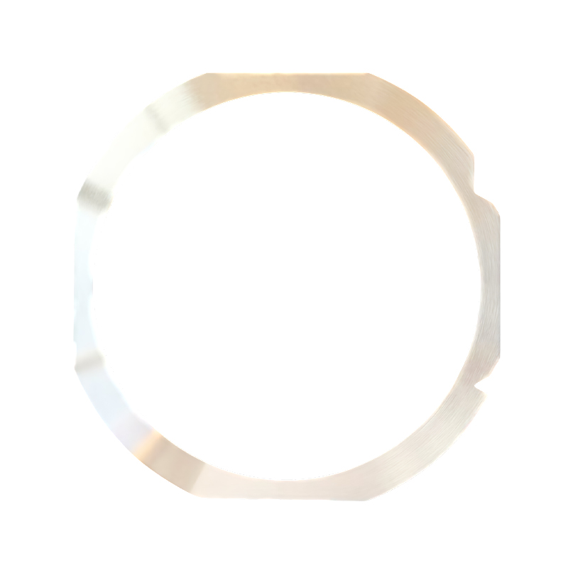
Modern wafer mounting plate design prioritizes ultra-high flatness and dimensional stability. For silicon wafers with diameters of 300mm or even larger, the surface flatness of the mounting plate typically needs to be controlled within the micrometer range to ensure uniform stress on the wafer throughout the process, avoiding edge focusing failures, uneven film thickness, or mechanical stress damage caused by warping. To achieve this goal, high-quality products utilize special alloys or ceramic matrix composites with low coefficients of thermal expansion. Through precision grinding, stress-relief heat treatment, and final polishing in an ultra-clean environment, internal residual stress and microscopic fluctuations are eliminated. Even during prolonged operation in high-temperature or vacuum environments, deformation remains minimal, ensuring process consistency.
Conductivity control is another key technical dimension. In certain plasma etching or electrostatic chuck (ESC) applications, mounting plates require specific conductive paths or grounding capabilities to effectively dissipate static charges accumulated on the wafer surface, preventing electrostatic discharge (ESD) damage to sensitive devices. In other scenarios, high insulation is required to avoid signal interference. This differentiated demand drives customized material and structural designs—for example, by locally embedding conductive layers, coating functional thin films, or adjusting the bulk resistivity to precisely match the electrical interface specifications of different device platforms.
The quality assurance system throughout the manufacturing process also reflects a high level of expertise. Advanced five-axis machining centers, laser interferometers, white-light interferometric profilometers, and coordinate measuring machines are used for end-to-end dimensional and geometric tolerance monitoring. Surface roughness, cleanliness (particle residue), and metal ion contamination are rigorously controlled using specialized testing equipment in a cleanroom environment. Each mounting plate undergoes multiple verifications before leaving the factory to ensure it meets SEMI standards or customer-specific technical agreements.
Furthermore, for emerging fields such as advanced packaging, compound semiconductors, and MEMS, wafer mounting plates must address more complex challenges—such as non-destructive clamping of thin wafers (<100μm), thermal compatibility with non-silicon substrates (such as GaAs and SiC), or integrated temperature sensing and feedback functions. This requires manufacturers to possess not only materials and process capabilities but also a deep understanding of downstream process mechanisms, providing end-to-end technical support from conceptual design and simulation analysis to small-batch verification.
In summary, wafer mounting plates are not ordinary metal plates but high-value-added functional components that integrate precision mechanics, materials science, and semiconductor process knowledge. Silently supporting the priceless wafer, it becomes an invisible guardian of stability, cleanliness, and precision in the battlefield of the nanoscale. When a wafer completes key processes on the mounting board and smoothly enters the next stage, beneath that seemingly calm surface lies a silent promise of "ultimate reliability" from countless engineering details.