
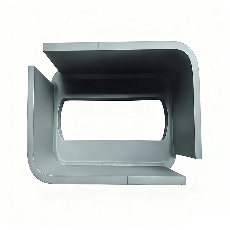


How can the layout of an electronic wafer mounting plate be optimized to reduce interference loss during signal transmission?
Release Time : 2026-01-12
As the core carrier connecting the chip to external circuits, the wafer mounting plate's layout design directly determines the quality and stability of signal transmission. In high-speed signal transmission scenarios, an unreasonable layout can easily lead to signal distortion due to reflection, crosstalk, and radiation loss, thus affecting chip performance and even causing system failure. Therefore, optimizing the wafer mounting plate layout requires a comprehensive approach across seven dimensions: signal partitioning, routing rules, grounding strategies, power planning, shielding design, material selection, and system coordination, to maximize signal integrity.
Signal partitioning and isolation is the primary principle of layout optimization. Wafer mounting plates typically integrate various types of signals, including analog, digital, high-frequency, and low-frequency signals, each with significantly different sensitivities to interference. For example, high-frequency signals are easily affected by switching noise from nearby digital signals, while analog signals are extremely sensitive to power fluctuations. Therefore, different types of signals need to be separated into independent areas, reducing coupling paths through physical isolation. Simultaneously, high-voltage and low-voltage areas must be clearly separated to prevent high-current signals from interfering with weak signals through spatial radiation or conduction paths, ensuring electromagnetic compatibility between signal areas.
Refined routing rules are key to reducing signal loss. High-frequency signal lines must adhere to the principles of "short, straight, and equal length" to minimize transmission path length and reduce dielectric loss, avoiding bends or forks that introduce parasitic parameters. For differential signals, consistent line width and spacing are essential to ensure common-mode rejection ratio and reduce signal distortion caused by mode conversion. Furthermore, traces should be kept away from board edges, connectors, and heat dissipation holes, and should avoid parallel routing with power lines to prevent crosstalk due to coupling effects. If crossing is unavoidable, perpendicular crossing or increased isolation distance should be used to reduce interference.
Grounding strategy is crucial for signal integrity. Wafer mounting plates should employ a multi-layer structure with a continuous, large-area ground plane to provide a low-impedance return path for signals and reduce ground loop interference. Dedicated grounding can be added to critical high-frequency areas, connected to the main grounding via independent vias to reduce local ground impedance. Simultaneously, signal loop area should be minimized, and differential pairs should be routed close to the ground plane to utilize the mirror effect to reduce radiation loss. For sensitive circuits, grounding vias can be added on both sides of the signal lines to form an electromagnetic barrier, further suppressing external interference.
Power supply planning directly impacts signal quality. Power lines and ground lines must be tightly coupled to form a low-impedance power distribution network, reducing the impact of voltage fluctuations on signals. Filter capacitors should be added to power inputs to suppress high-frequency noise, and parallel routing of power lines and signal lines should be avoided to prevent coupling interference. For multi-power systems, power plane partitioning should be rationally planned according to current requirements to ensure stable power supply in each area and reduce cross-area interference. Furthermore, power and signal layers should be arranged alternately to utilize interlayer capacitance for further filtering.
Shielding design is an effective means of suppressing external interference. For high-frequency sensitive devices, such as crystal oscillators and RF modules, metal shielding covers should be added to block spatial radiation interference. Critical signal lines can be wrapped with grounded copper foil to form a transmission line shielding structure, reducing electromagnetic leakage. For multilayer boards, inner layer signal lines should avoid overlapping with power or ground layers to prevent signal attenuation due to dielectric loss. Simultaneously, grounding via arrays should be set at the board edges to form a Faraday cage effect, shielding external electromagnetic fields.
Material selection and process coordination must be integrated with the layout design. High-frequency substrates such as PTFE or ceramic substrates have low dielectric loss characteristics, which can reduce dielectric absorption loss during signal transmission. Soldering and cleaning processes must avoid residual metal debris or cold solder joints to prevent signal reflection caused by localized conductivity anomalies. Furthermore, surface treatments such as immersion gold or chemical gold plating can improve pad flatness, reduce the impact of contact resistance on high-frequency signals, and ensure signal transmission continuity.
System-wide collaborative design is the ultimate goal of layout optimization. The wafer mounting plate layout must be coordinated with the overall system, considering interface layout, connector matching, and EMC compatibility. For example, high-speed interfaces should be kept away from interference sources, and their layout direction should be consistent with the signal flow direction to reduce transmission delay. Regularly linking signal integrity simulation with prototype testing can identify layout defects early, such as impedance discontinuities and excessive crosstalk, and eliminate potential risks through iterative optimization, ultimately achieving high performance and high reliability for the wafer mounting plate.